HDI PCBs — Understanding Advantages & Applications
With so many different types of printed circuit boards on the market, it can be a challenge to determine which one is right for your next project. In this post, we explore one of the more common choices — the high density interconnect PCB.
What is an HDI PCB?
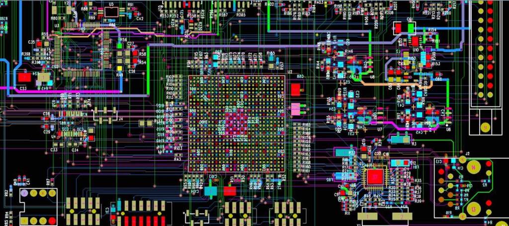
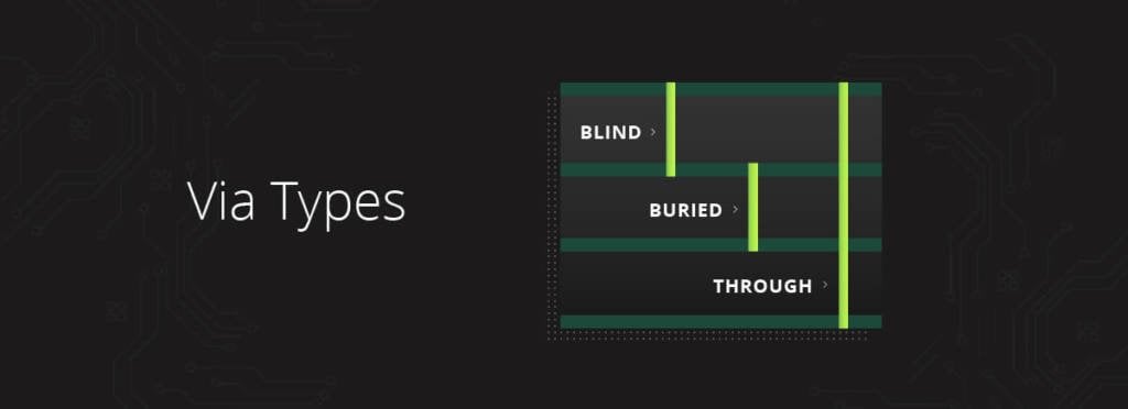
HDI PCBs are characterized by thin lines, closer spaces, and more dense wiring, which allow for a faster connection while reducing the size and bulk of a project. These boards also feature blind and buried vias, laser-drilled microvias, sequential lamination, and via in-pads.
HDI vs. Standard PCBs — What’s the Difference?
HDI PCBs provide better signal integrity and have a higher layer than standard PCBs. They also lead to higher density (and therefore smaller) PCBs.
HDI PCBs feature laser micro vias while standard PCBs only have mechanical drilling.
In addition, ball grade arrays (BGAs) are defined by numbers of pins (or connections) that are attached to the board. As the pin count increases, you will require a micro via in-pad nearly 100% of the time.
HDI PCB Applications
HDI PCBs are used in a wide variety of applications, including:
- Electronics in the auto industry (navigation, GPS, etc.)
- Smartphones and cell phones
- Tables
- Laptops
- Game consoles
- Wearable technology (Apple watch, fitness trackers, etc.)
- Military and aerospace
- Telecommunications
Benefits of HDI Printed Circuit Boards
Whether you should have an HDI PCB is typically up to the designer. Benefits of this type of board include:
- Versatility
- Cost-effective
- Reliability
- Better signal integrity/high speed (you get more in this circuit board package as opposed to having to use multiple PCBs)
- Better signal
- Compact design
- High frequency
HDI Via In-Pad Fill Process
This refers to a specialized copper plating process. It differs from the via in-pad fill process for non-HDI, standard PCBs.
HDI Lamination & Materials Process
Questions About HDI PCBs?
We have the experience and knowledge to take on all complex PCB jobs — including HDI fabrication and manufacturing. As one of the leading HDI PCB manufactures, we continue to invest in the most sophisticated production and testing technology. We also have the deep engineering experience to handle all types of jobs with incredible accuracy — on time and on budget.
If you’re looking for more information please contact us or visit our HDI PCB page to learn about our capabilities, fabrication tolerance, certifications, and more.


